-
Mail Us Todaysales@efpcb.com
-
Company LocationShenzhen, Guangdong, China
-
+86-755-23724206Call us for more details
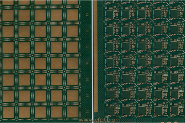
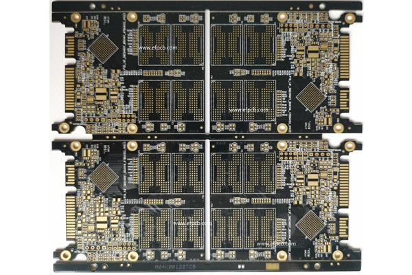
Layer count: 6L HDI PCB
Material: FR4 , 1.0 mm, High TG, 0.5 OZ for all layer
Minimum tack: 2.8 mil
Minimum space(gap): 2.8 mil
Minimum hole: 0.15mm
Surface finished: ENIG
Panel size: 220*268mm/4up
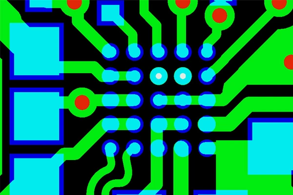
Characteristics: high density interconnect PCB, via on pad(plug with resin, copper capping), high TG, thin core 3mil thickness
High-Density Interconnect (HDI) PCB is a significant part of the modern electronics revolution, providing dense, high performance solutions for higher technology applications. As the trend for smaller and faster devices ramps up demand, HDI PCB design is essential in the electronics industry. This ultimate guide will take you to learn the production process, design factors as well as intrinsic matters on the topic of HDI PCB, which help you to have a clear picture of this advanced area.
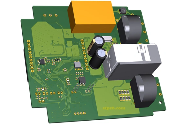
HDI PCB layout is used in the creation of printed circuit boards that contain high density of components and interconnections. Unlink conventional PCBs, HDI PCBs apply finer lines, smaller vias and more layers to stuff more elements in smaller space. That makes them suitable for uses like smartphones, wearables, medical devices, auto, and AI computing.
The primary characteristic of HDI PCB is as follows:
As electronics continue to be more and more integrated, HDI PCB design is a necessity to meet the requirements of today's and future technologies. From $13.6 billion in 2023, the HDI PCB market around the world is expected to reach $18.8 billion in 2028 by market research company MarketsandMarkets, due to the adoption of 5G, IoT, and AI innovations.
The ability to fit more functions in same or less space without sacrificing performance that´s the true benefit of HDI PCB. From making it possible for 5G devices to transmit signals at record speeds to serving as interconnect for AI systems running the most complex processing, HDI PCB design is driving the future of electronics.
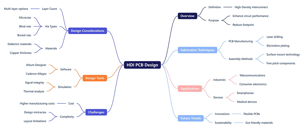
The selection of materials used in the fabrication of HDI PCB is very crucial in realizing performance and reliability. Common materials include:
Materials are selected based on purposes as choosing the right one for the application, operation environment and signal requirements.
HDI PCB fabrication takes place over many complex steps that must be done with precision and state-of-the-art tech. A detailed description of the manufacturing is given hereinafter:
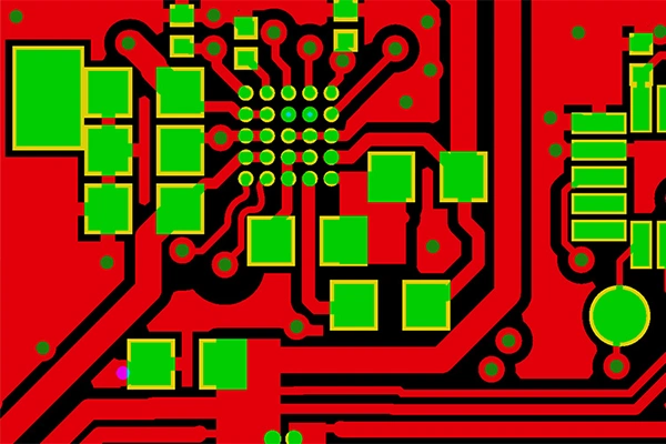
Before we can even begin to make an HDI PCB, we have to start the circuit design process. Advanced CAD tools such as Altium Designer or Cadence Allegro would be used by an engineer to construct a design, taking into account things like:
Simulations are usually carried out to verify the design and to anticipate possible issues prior to production.
HDI PCBs are generally multi-layered boards that are layered in lamination to produce a relatively dense package. The lamination process involves:
Microvias, blind vias and buried vias are among the key attributes of HDI PCBs. These are made using sophisticated drilling methods like:
Following the drilling, when the vias are copper-plated to provide electrical connection among the layers. This step is referred to as an electroless copper deposit.
The unwanted copper is removed using etching process of the board, then circuit patterns are formed. A photoresist is then applied to the board and the pattern is exposed on it by UV light. Exposures are etched away (chemically), forming delicate lines and spaces.
Accuracy is essential here, as HDI PCBs need highly detailed line widths and spacing.
The copper traces are then covered with a solder mask to shield them from oxidation and avoid short circuits during assembly. The solder mask is green usually however other colors can be created. The solder mask is applied through a process of printing on the board using screen printing and curing by UV light or heat.
The surface finish protects the board from environmental exposure, thus increasing the board’s overall longevity and solderability. Some finishes which are popularly used in HDI PCB design are:
The particular surface finish selected will depend on the cost, application demands, and environmental concerns for the wood floor in question.
The HDI PCB should be tested for function when before being shipped to the customer. Common tests include:
The last stage of the production process is a complete board inspection where the board is checked against design specifications and quality standards. AOI (Automated Optical Inspection) and X-ray inspection are the more sophisticated methods used to identify non-visible suggestions of imperfections. Applications of HDI PCB Design
High density interconnect PCBs are applied in the following fields:
The flexibility in HDI PCB layout makes it essential for high-performance and small form factor industries.
What are the major advantages of HDI PCB design?
Advantages of HDI PCB design HDI PCB design has many benefits such as:
What is the different in HDI pcb design and normal PCB design?
HDI in PCB design uses thinner lines, smaller vias, and more layers vs conventional PCB designing. Thus, more components and interconnect literally can be placed in a smaller space, so HDI PCBs are excellent for highly dense, complex circuit boards.
What kind of problems are there in HDI PCB production?
Some of the challenges are tight alignment during lamination, accurate laser drilling of micro vias and signal quality in high densities designs. It is these challenges which can only be met through advanced production methods and very strict quality control.
How we can help you optimize your HDI PCB design?
To improve your HDI PCB design:
Is HDI PCB design cost-effective?
Although HDI PCBs are more expensive than other types because of the more complicated manufacturing process, they are small in size, high in capabilities, and reliable, thus making them a cost-effective option in the long run.
HDI PCB design is a fundamental element of the modern electronics industry as it permits the manufacture of small, high-speed products that the current fast-paced, technologically driven environment calls for. From smart phones to high end computing HDI PCB have become necessary. You can use HDI PCB design to design innovative solutions that will enable and define what can be achieved in 2025 and beyond by understanding some of the basics of how they’re built, what to consider in your designs, and trends in the industry.