


IC Substrate | Comprehensive Guide (2021)
The IC substrate (also called the IC packaging substrates) is a critical common element utilized in innovative processing to assemble bare IC (integrated circuit) devices. Through a conducting system of cables and holes, the IC substrates serve as a link between the IC chip and the PCB. IC stands for intermediary products, and it serves multiple aims:
- Take a photo of a semiconductor's IC chip.
- Internally wire connects the chip to the PCB.
- This could shield, reinforce, and sustain an IC chip while also acting as a heat sink.
- Classification of transmission and energy.
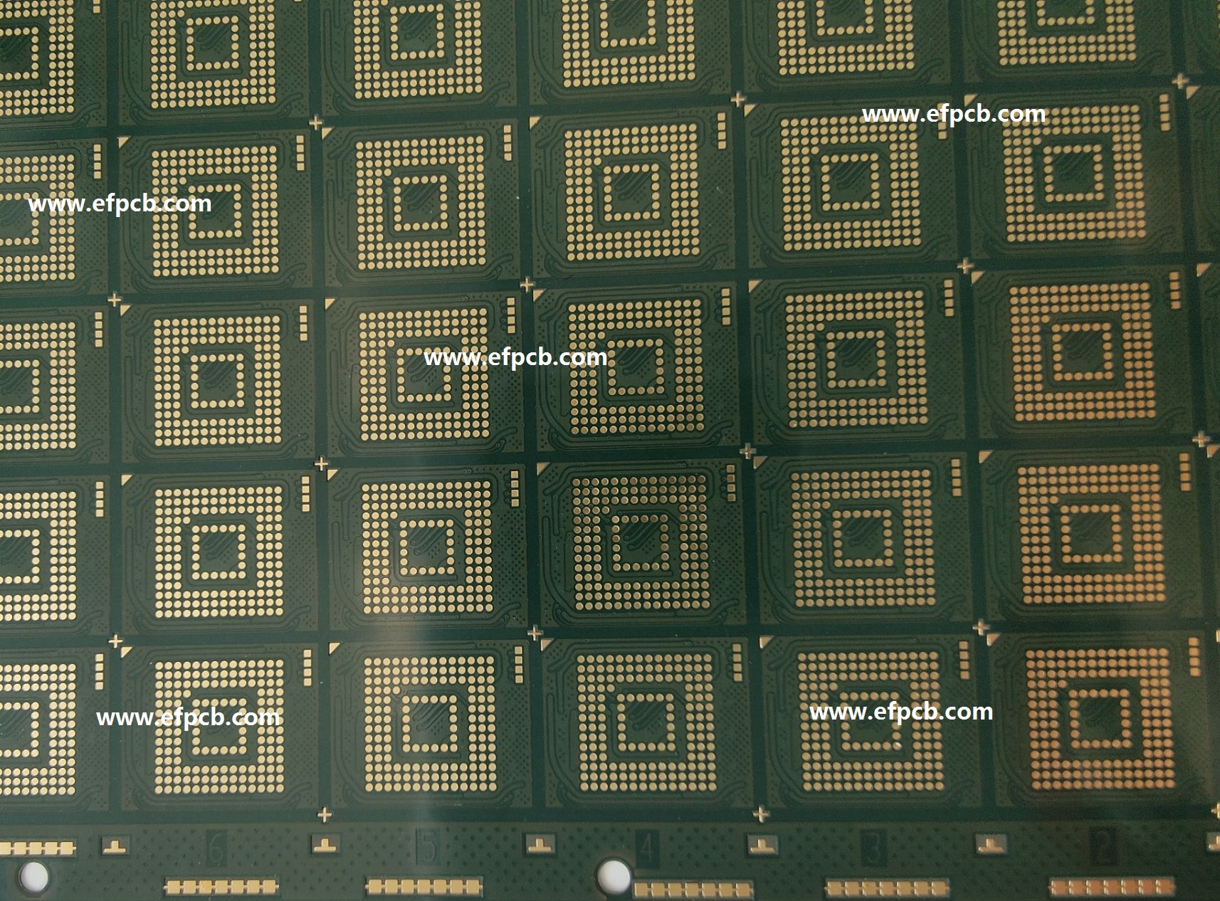
Due to a broad system of conducting traces and holes, IC substrate provides contact between your IC chips and the printing circuit boards. The functionality, circuitry assistance, security, signal distribution, power management, and heat transfer of your PCB have all been dependent on the substrates.
Within that type of production, IC packaging substrate seems to be the pinnacle of downsizing and depends on procedures comparable to semiconductors production. A range of methodologies, such as flip-chip procedures and wires binding, could be used to attach IC chips to your boards via the IC package substrate.
IC substrate has already been growing, thanks to the advancement of BGA (ball grid array) & CSP (chip-level packing) as well as other innovative ICS, and all these ICs require additional packing materials. IC PCB, including any level of HDI PCB and flexibility rigidity PCB, has exploded in demand and use as among the most modern PCBs (printing circuit boards). It was becoming commonplace in telecommunication and digital news.
Formation of IC Substrate
Traditional integrated circuit (IC) packing, including a two-sided pin flat packaging, four-sided pin flat bundle, and so on, utilize a leads framework as the substrates for the IC conductivity lines and sustaining IC, with interconnecting pins on both ends or across the leads frames. That packing solution could also fit the standards if the amount of current isn’t too high. The fundamental length of an IC is shrinking as semiconductors technology develops, and the level of correlation keeps increasing.
The relevant integrated circuit package is going down the path of ultra-multi-pin, thin pitch, and ultra-downsizing. The standard leading package hasn't been capable to keep up with the demands.
Classification of IC Substrate
- As previously stated, package substrate can be classified in a variety of ways, including packaging technique, materials qualities, and research areas.
- Wire bonding packing substrates and flip-chip package substrates are two types of packaging substrates that are used in different packaging procedures.
- Package substrates are classified as rigid boards, flexible PCB, or ceramics substrates based on the material used.
- Computer chip products substances, MEMS packaged food substances, RF module packaged substances, processor chip packaged substrates, and high information packaged sorbents are some of the most common types of packaged substrates were using in smartphone intelligent stations, services/storage, and other applications.
- Materials for BGA integrated circuits. The IC substrate has excellent heat dispersion and electricity efficiency, and it could accommodate a large number of chip pins. As a result, it can be used in IC packaging with even more than 300 pins.
- Substrates for CSP IC. CSP is a single-chip packaging that is light, compact, and identical to IC in mass and dimensions. Memory devices, communications devices, and electronics items with a minimal amount of memory are all common uses for CSP IC substrates.
- Support for FC IC. A flip-chip component with lower spectral interfering, low circuit losses, great performance, and efficient heat transfer has been known as FC (flip chip).
Manufacturing of IC Substrate
First or foremost, we must comprehend three distinct PCB manufacturing methods. There are three types of PCB and IC substrate manufacture methods now available:
- Subtractive processing (SP)
- Additive process (AP),
- Modernized semi-additive procedure (MSAP)
Subtractive Processing (SP):
Its most basic PCB manufacturing method, which involves plating specified thicknesses of copper foil on the copper-clad laminate, then protecting the circuitry and through it with a dry coating, then eliminating the unneeded copper sheets. The main disadvantage of such a procedure is that the backside of the copper foil would also be inscribed during etched operation. Because side etches exist, the minimal line width/spacing of a PCB can only be higher than 50 m (2 mils), limiting it to certain standard PCB, FPC, and HDI devices.
Additive Processing (AP):
The circuitry will be first placed on an insulating layer including photographic catalysts, and afterward selected chemicals copper depositing was performed on the uncovered thick circuits to produce a full PCB. Because this approach does not require subsequent etching, it can attain extremely high reliability and production times of less than 20 m. The aim will be achieved further used manufacture WB or FC IC substrates, and its procedure could approach 12 M / 12 M. It has demanding importance for substrates and system requirements, increased price, and poor productivity; these are primarily often used to create WB or FC IC substrate, as well as its processing could achieve 12 M / 12 M.
Modernized semi-additive procedure (MSAP):
Initially, narrow copper material is electroplated on the copper-clad laminate, if the places that don't have to be electroplated were also shielded, then electroplated and then covered with such an anti-corrosion covering, and finally, the most inorganic copper surface is separated by lightning etching, removing the necessary copper surface line. So because the copper coating has become so narrow at the start of the electroplating process, flashing corrosion occurs quickly, and sides corrosion does have a minor impact.
The MSAP process, which is the most prevalent fine circuit boards method of manufacture, offers the benefits of large yields with cheap manufacturing costs when contrasted to the subtracting and adding methods. CSP, WB, and FC IC substrates, as well as other finer line substrates boards, are manufactured and use this technique. Even though the SLP (substrate-like PCB) is a printable circuits boards, its minimal line width/line separation from a processing standpoint is 30 M / 30 m, and therefore it cannot be created using the subtracting approach, and MSAP processing technologies are developed.
The IC substrate's technological hurdles
The IC substrates boards have various technological challenges as contrasted to a regular PCB. Those technical challenges are the most significant barrier to entry for IC substrates boards in the business. The preceding is a list of IC substrates board engineering hurdles.
- Core board production equipment: the IC substrates board's basis boards were extremely slim and easily deformed. Warpage and laminating thicknesses of ultra-thin core boards could only be properly managed when processing method such as boards’ expansions and compression, laminating factors, and so on has made the breakthrough.
- Microvia innovation has a micro via dimension of around 30 m, which is much smaller than standard PCB and HDI, and a variety of stacking levels of 3, 4, and 5 levels.
- Patterned formation and copper plating technique necessitate excellent copper plated thicknesses accuracy and fine circuits flash eroding. The current line width separation standard is 10-30 M. Copper plated thicknesses consistency ought to be 18 3 m, and etch uniform ought to be 90 percent.
- The soldering masking area of the IC substrates has a difference in height of less than 10 m, and the difference in height among the soldering masks and the pads was even less than 15 m.
- Product dependability test methodology and assessment capabilities IC substrate factories must be equipped with various testing equipment/instruments not found in traditional PCB factories, as well as master reliability testing technologies not found in conventional PCB factories.
The MSAP technique is used to make IC substrates, which is a complicated procedure. In general, the minimal line width/spacing of an IC substrate would be less than 30 M. The classic subtracting technique has struggled to match the IC substrate's needs. MSAP is by far the most prevalent method for fabricating IC substrates.
IC substrates panel's environmental conservation barriers
The obstacles to entry into the IC substrate sector are considerable, and they aren't just technological. High technical demands and various patent limitations have produced a high hurdle to entry for the IC substrate sector, which also includes investment and consumers as impediments.
The initial R & D expenditure is large and time-consuming because of the strong technical challenges of IC substrates boards, and the project's developmental risk is significant. The development and additional mental of an IC substrate board manufacturing line necessitate a significant capital investment, the largest of which being initial investor in machinery.
The substrates of boards were comparable to that of a copper-clad lamination on a PCB, and it is separated into three categories: hard substrate, flexibility films substrate, and co-fired ceramics substrate. The tough and flex substrates offer more proposed projects whereas the co-fired ceramic substrate has a lower level of progress. Impact strength, high-frequency properties, heat tolerance, and thermally conductance are the most important characteristics of IC substrates.
The most expensive part of IC packaging is the substrate, which accounts for more than 30% of the total. Packaging substrate, packaging materials, machine degradation, and tests are all included in the cost of IC packaging.
EFPCB is the market leader and expert in the PCB design industry. Interested to know more about IC substrates, just write us now at sales@efpcb.com.

- Skype Id: shawnwang2006
- Phone no.: +86-755-23724206
- Email: sales@efpcb.com
- Quick Contact