Know About Printed Circuit Board Manufacturing Process
Keywords: Printed Circuit Board Manufacturer, PCB Manufacturer, PCB Manufacturing
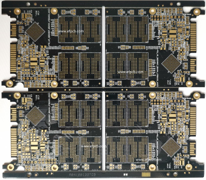
During the fabrication process, for the extra layers of the design, there is a requirement of additional steps which are provided by multilayer printed circuit boards. They copy a few steps that were used during single-layer PCBs. However, the phases are repeated in each layer of the board. In multilayer PCBs, copper foil replaces the copper coating that is present between the layers. PCB Manufacturing is a process that is done with utmost accuracy.
Circuits Board Inner Layer Imaging
Inner layer imaging undergoes a procedure that is very much similar to the printing of PCB design. The designs are printed on a plotter printer so that a film can be created. The solder mask present in the inner layer gets printed out. After their alignment, a registration hole is created by a machine in the films so that later the films are lined up properly with the layers intact.
Technicians place the printed film over the laminate and align them with the help of registration holes.
Printed Circuits Inner Layer Etching
After the process of imaging is completed, they are covered with the hardened white ink. The copper which is present beneath is protected by this hardened material which will remain on the board after etching.
To remove any remaining resist from the board that didn’t harden, technicians first wash off the board with the use of alkaline. Through this cleaning, some areas are exposed that were initially covered. Then PCB Manufacturer etches off the excess copper by submerging the board into a copper solvent.
It Resists Stripping
The role of resist stripping is that it removes any remaining resist that covers the copper of the PCB inner layer. Cleaning the left-out resist will make sure that the copper now cannot hamper its conductivity. After the resists are removed, the layer is ready to go through the inspection of its basic design.
Layup
In the multilayer PCB fabrication, the layup step process takes place and it happens when a machine provides its help to line up, heat, and bond the layers together with a copper foil layer and insulating material that is present in between the inner and outer layers. Computers guide these machines because there should be a proper alignment of the layers and for the printed circuit board’s proper structure the bonding has to be exact. Printed Circuit Board Manufacturer performs this process by keeping everything in mind.
- 1Understanding UL 94V-0 Flammability Rating for Printed Circuit Boards (PCBs)
- 2HDI PCB Market Outlook 2025: Future Prospects, Growth Analysis & Innovations
- 3HDI PCB Design Comprehensive Guide: Mastering High Density Interconnect Technology in 2025
- 4Top 10 Flexible PCB Factories in 2025
- 5Top HDI PCB Manufacturers (2024)
- 6IC Substrate | Comprehensive Guide (2021)
- 7PCB core raw material CCL
- 8How to Make mSAP PCB?
- 9Top 10 IC Substrate Fabricators (2024)
- 10What is IPC 4761 Type VII Via in Pad PCB?

- Skype ID: shawnwang2006
- Phone No。: +86-755-23724206
- Email: sales@efpcb.com
- Quick Contact